By Frank Bowman, President, Niche Electronics
In our typical articles, we try to offer information about our processes, our commitment to service, and
trends in the marketplace. But sometimes, we take for granted that people who are new to printed
circuit boards are familiar with our industry’s terminology.
With that in mind, we’ve compiled ten terms you’re likely to come across, and added a few simple
definitions that show how they relate to the overall printed circuit board process:
1. PCB
Printed Circuit Board
2. PCBA
Printed Circuit Board Assembly
While these two terms are often used interchangeably, there is a slight difference.
The process of populating a bare board with electronic components via soldering is called assembly, so a
PCB refers to something that is pre-assembly — a bare board with lines, holes and pads that connect
various points. The PCBA refers to a completed, post-assembly, printed board with the components in
place.
3. Gerber Files
These are an electronics industry data file format for communicating design information to
manufacturers of PCBs.
4. BOM – Bill of Materials
The list of components, their quantities, their sourcing data, and reference designators on the PCBA.
5. Wave Solder vs. Selective Solder
Wave Solder is an automated soldering process using a tray or pan of molten solder, raised by a pump to
contact the PCB, to attach electronic components.
Selective Solder is the process of soldering only very specific components to PCBs that might be
damaged by the heat of a reflow oven or wave soldering techniques.
6. SMT – Surface Mount Technology
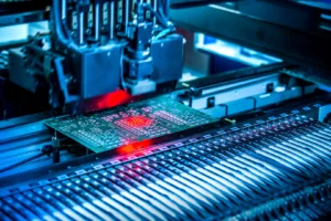
Surface Mount Technology (SMT) uses a broad, automated soldering process to affix components onto
the top surface of a PCB. These components are usually mounted by pick-and-place machines and
soldered into place using a reflow oven.
7. Thru Hole Mounting Technology
In contrast to SMT, Thru-Hole mounting involves placing the leads of electronic components through a
plated hole in the PCB and then soldered on the bottom surface of a PCB.
8. No-Clean vs. Aqueous-Cleaning Processes
To better help in the soldering process, a PCB assembly process incorporates a cleaning agent known as
flux to prevent contamination and oxidation on the boards. Once a PCB’s components are affixed, the
remaining flux may or may not be cleaned off, depending on the way in which the components were
soldered, and the type of flux. “No Clean” and “Aqueous Clean” are two ways of dealing with this flux
after the assembly is completed.
A No Clean Process uses a type of low-residue flux that can, in most cases, be left on the PCB board after soldering is completed without compromising the performance of the PCB.
An Aqueous Clean Process is used following a soldering process that employs a paste made up of a more water-soluble flux. This flux is more sensitive and reactive to exposure to water once the board is added to the finished product. This makes it necessary to completely remove excess flux residue by an automated washing of the PCB boards with distilled water.
9. RoHS Compliance- Restriction of Hazardous Substances
RoHS Compliance is a European Union directive that restricts the use of ten hazardous materials (such as lead) that are found in some electronic and electrical equipment to reduce occupational exposure during manufacturing and reduce toxic electronic waste.
10. AOI -Automated Optical Inspection
AOI refers to a tool that has far more sensitive receptors than the human eye, and which can visually inspect a PCBA for bad soldering or other assembly errors.
It may seem simple, but product developers with a basic understanding of these terms may be better
equipped, and more confident, to talk about making their ideas a reality.
If you have questions about these or any other terms, let us know. We’re happy to help.

